 The emergence of Additive Manufacturing (AM) has been fueled by its ability to transform digital designs into physical objects. Unlike conventional manufacturing techniques, which involve complex tooling and machining processes, AM builds objects layer by layer using materials such as plastic, metal, and ceramics, based on digital designs.
Over the years, significant advancements in AM technology have transformed the production of numerous components. The rise of the DLP (Digital Light Processing) AM method, in particular, has been driven by its ability to fabricate parts with unparalleled precision and accuracy. By harnessing the power of digital light projection, this technique offers enhanced control over the manufacturing process, enabling the creation of complex geometries and customizable designs that were previously unimaginable.
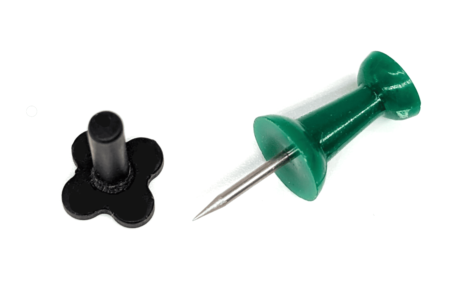
ESD components play a vital role in various industries, especially in electronics and telecommunications, where the protection of sensitive equipment from static charges is crucial. In today’s rapidly evolving technological landscape, the demand for miniature electronic components is steadily increasing. To meet this demand, manufacturing processes with the capability to produce components with enhanced electrostatic discharge (ESD) protection and intricate features, while also offering cost and time savings, are crucial.
Traditionally, micromachining has been the go-to method for creating these components. With the advent of DLP AM, manufacturers now have a superior alternative that offers numerous advantages. In this article, we will explore the capabilities of DLP in the realm of manufacturing miniature ESD components, as well as the cost and time-saving benefit it brings to the table.
To download the white paper, click the button below. To learn more about Mechnano’s technology and ESD materials options for AM, contact us at info@mechnano.com.